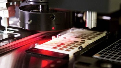
InP AND GaAs Technologies
All of the key processes which are necessary to design & manufacture high-technology GaAs and InP optoelectronic chips are contained under one single roof in Nozay, within the Paris-Saclay high-tech valley.
This manufacturing plant regroups the following capabilities, for both technologies :
![]() Product design
Product design
![]() MOPVE and GSMBE epi-wafer growth
MOPVE and GSMBE epi-wafer growth
![]() Front-end and back-end processing
Front-end and back-end processing
![]() Testing
Testing
![]() Reliability demonstration and product qualification
Reliability demonstration and product qualification
Having the technological and physical capability to handle all of these manufacturing elements provides significant advantages to 3SP Technologies customers: shorter lead times, better cost control, shorter development cycles and state-of-the-art products.
